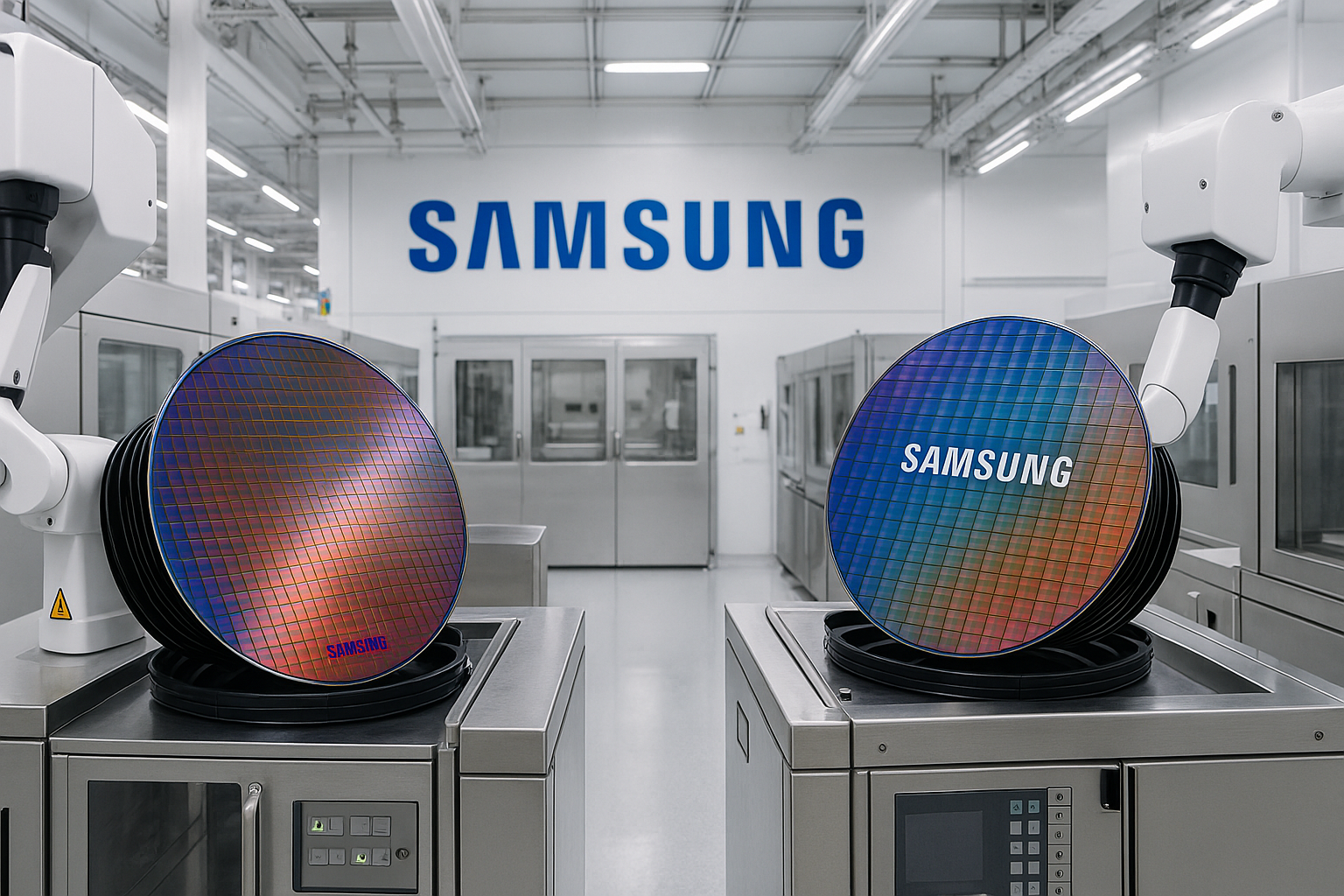
Samsung has officially formed a team to develop 1 nm process technology, marking the next step following its ongoing efforts with 2 nm GAA architecture.
According to Sedaily, the new phase is referred to within the company as “the semiconductor industry’s dream.” Mass production of such chips is planned for 2029.
Transitioning to 1 nm will require new-generation EUV lithography equipment with high numerical aperture (high-NA EUV). It’s unclear whether Samsung has placed an order for this equipment, which is essential for the project’s success.
Meanwhile, competitors are also making progress. TSMC has started accepting orders for 2 nm chips and is working on 1.4 nm process technology. Samsung, for its part, has achieved approximately 30% yield on test 2 nm production — better than its 3 nm process, though still far from maturity.
Previously, reports suggested that Samsung might halt work on 1.4 nm technology to focus on 2 nm. Now, however, attention has shifted to a more ambitious goal — 1 nm.
If everything goes as planned, the Korean company could take the lead in the race for ultra-compact transistors.


